Taming terahertz: MIT’s new chip design breaks through silicon barriers – Interesting Engineering
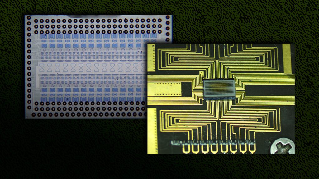
Terahertz waves can revolutionize the internet, healthcare, and airport security. Here’s how a tiny chip can finally allow us to use them.18 hours ago19 hours agoa day agoa day agoa day ago2 days ago2 days ago2 days ago2 days ago2 days ago7 minutes agoan hour ago15 hours ago15 hours ago16 hours ago16 hours ago18 hours ago19 hours ago20 hours ago21 hours agoRupendra BrahambhattThe new chip design developed by the MIT team.Source: MIT NewsHumans have figured out many ways to utilize radio waves, X-rays, microwaves, infrared light, and many other types of electromagnetic radiation. However, terahertz waves remain an unsolved puzzle.Scientists have known about terahertz waves for years. Their unique properties suggest that these waves could enable high-bandwidth communication, ultra-fast data transfer, advanced medical imaging, and precise environmental monitoring. Additionally, their ability to penetrate various materials without harmful radiation makes them valuable for security screening, quality control in industries, and chemical sensing. However, until now, it has been challenging to harness the potential of these waves in electronic devices due to several technological limitations.Finally, a new study from researchers at MIT reveals a chip-based solution that can overcome these limitations and make terahertz waves more accessible than ever.Terahertz (THz) waves are affected by the dielectric constant, a measure of how well a material can store and slow down an electric field. The lower this constant is the smoother terahertz waves can pass through a material.Unfortunately, silicon which is a key material in chips and electronic circuits has a high dielectric constant. “Because the dielectric constant of silicon is much higher than that of air, most terahertz waves are reflected at the silicon-air boundary rather than being cleanly transmitted out the back,” the study authors said.A common approach to improve THz wave transmission is to use silicon lenses, which focus and enhance wave power. These lenses not only generate terahertz waves but also boost their radiating power allowing them to cover long distances.However, there’s a catch. Due to their size and cost, silicon lenses can’t be integrated with electronic chips. Therefore one can’t use terahertz waves generated by these lenses for data transfer or any other electronic purpose.“Such (silicon) lenses, which are often larger than the chip itself, make it hard to integrate the terahertz source into an electronic device,” the study authors said.The MIT team developed a new method to improve how terahertz (THz) waves pass through silicon chips. As mentioned earlier, a significant portion of these waves gets reflected due to a mismatch between the properties of silicon and air, leading to signal loss. To address this, the researchers applied a principle called matching, which involves reducing the difference between silicon (dielectric constant is 11) and air (dielectric constant is 1) so that more waves can travel through.They first placed a thin sheet of material at the back of the chip. This sheet had properties that helped bridge the gap between silicon and air, allowing more waves to pass through rather than being reflected.Next, they used a laser cutter to create microscopic holes in the sheet, adjusting its properties so that it matched the THz waves more effectively. Finally, they incorporated high-frequency transistors, developed by Intel, which improved the generation and transmission of THz waves.“These two things taken together, the more powerful transistors and the dielectric sheet, plus a few other small innovations, enabled us to outperform several other devices,” Jinchen Wang, lead study author and a graduate student, said.This new design led to stronger and more efficient THz signals compared to existing methods. “The chip generated terahertz signals with a peak radiation power of 11.1 decibel-milliwatts, the best among state-of-the-art techniques. Moreover, since the low-cost chip can be fabricated at scale, it could be integrated into real-world electronic devices more readily,” the MIT team notes.However, creating a terahertz beam requires not just one but many such chips. The next step for the researchers is to scale their method to produce a large number of chips.The study will soon be presented at the IEEE International Solid-State Circuits Conference (ISSCC).Rupendra Brahambhatt Rupendra Brahambhatt is an experienced writer, researcher, journalist, and filmmaker. With a B.Sc (Hons.) in Science and PGJMC in Mass Communications, he has been actively working with some of the most innovative brands, news agencies, digital magazines, documentary filmmakers, and nonprofits from different parts of the globe. As an author, he works with a vision to bring forward the right information and encourage a constructive mindset among the masses.Stay up-to-date on engineering, tech, space, and science news with The Blueprint.By clicking sign up, you confirm that you accept this site’s Terms of Use and Privacy Policy2 days ago2 days ago2 days ago2 days agoPremiumIE PROFollow
Source: https://interestingengineering.com/science/mit-chip-unleashes-terahertz-waves